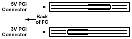
PCI Bus 32 BIT 5V 3V
| Pin No. | Signal Name | Pin No. | Signal Name | |
| A1 | Test Logic Reset | B1 | -12 VDC | |
| A2 | +12 VDC | B2 | Test Clock | |
| A3 | Test Mde Select | B3 | Ground | |
| A4 | Test Data Input | B4 | Test Data Output | |
| A5 | +5 VDC | B5 | +5 VDC | |
| A6 | Interrupt A | B6 | +5 VDC | |
| A7 | Interrupt C | B7 | Interrupt B | |
| A8 | +5 VDC | B8 | Interrupt D | |
| A9 | Reserved | B9 | PRSNT1# | |
| A10 | +V I/O * | B10 | +V I/O * | |
| A11 | Reserved | B11 | PRSNT2# | |
| A12 | Ground or Key * | B12 | Ground or Key * | |
| A13 | Ground or Key * | B13 | Ground or Key * | |
| A14 | Reserved | B14 | Reserved | |
| A15 | Reset | B15 | Ground | |
| A16 | +V I/O * | B16 | Clock | |
| A17 | Grant PCI use | B17 | Ground | |
| A18 | Ground | B18 | Request | |
| A19 | Reserved | B19 | +V I/O * | |
| A20 | Address/Data 30 | B20 | Address/Data 31 | |
| A21 | +3.3 VDC | B21 | Address/Data 29 | |
| A22 | Address/Data 28 | B22 | Ground | |
| A23 | Address/Data 26 | B23 | Address/Data 27 | |
| A24 | Ground | B24 | Address/Data 25 | |
| A25 | Address/Data 24 | B25 | +3.3VDC | |
| A26 | Initialization Device Select | B26 | Command/Byte Enable 3 | |
| A27 | +3.3 VDC | B27 | Address/Data 23 | |
| A28 | Address/Data 22 | B28 | GND | |
| A29 | Address/Data 20 | B29 | Address/Data 21 | |
| A30 | Ground | B30 | Address/Data 19 | |
| A31 | Address/Data 18 | B31 | +3.3 VDC | |
| A32 | Address/Data 16 | B32 | Address/Data 17 | |
| A33 | +3.3 VDC | B33 | Command/Byte Enable 2 | |
| A34 | Frame | B34 | Ground | |
| A35 | Ground | B35 | Initiator Ready | |
| A36 | Target Ready | B36 | +3.3 VDC | |
| A37 | Ground | B37 | Device Select | |
| A38 | Stop Transfer Cycle | B38 | Ground | |
| A39 | +3.3 VDC | B39 | Lock bus | |
| A40 | Snoop Done | B40 | Parity Error | |
| A41 | Snoop Backoff | B41 | +3.3 VDC | |
| A42 | Ground | B42 | System Error | |
| A43 | Parity | B43 | +3.3 VDC | |
| A44 | Address/Data 15 | B44 | Command/Byte Enable 1 | |
| A45 | +3.3 VDC | B45 | Address/Data 14 | |
| A46 | Address/Data 13 | B46 | Ground | |
| A47 | Address/Data 11 | B47 | Address/Data 12 | |
| A48 | Ground | B48 | Address/Data 10 | |
| A49 | Address/Data 9 | B49 | Ground | |
| A50 | Ground or Key * | B50 | Ground or Key * | |
| A51 | Ground or Key * | B51 | Ground or Key * | |
| A52 | Command/Byte Enable 0 | B52 | Address/Data 8 | |
| A53 | +3.3 VDC | B53 | Address/Data 7 | |
| A54 | Address/Data 6 | B54 | +3.3 VDC | |
| A55 | Address/Data 4 | B55 | Address/Data 5 | |
| A56 | Ground | B56 | Address/Data 3 | |
| A57 | Address/Data 2 | B57 | Ground | |
| A58 | Address/Data 0 | B58 | Address/Data 1 | |
| A59 | +V I/O * | B59 | +V I/O * | |
| A60 | Request 64 bit | B60 | Acknowledge 64 bit | |
| A61 | +5 VDC | B61 | +5 VDC | |
| A62 | +5 VDC | B62 | +5 VDC | |
| START OF 64bit CONNECTOR | ||||
| A63 | Ground | B63 | Reserved | |
| A64 | Command/Byte Enable 7 | B64 | Ground | |
| A65 | Command/Byte Enable 5 | B65 | Command/Byte Enable 6 | |
| A66 | +V I/O * | B66 | Command/Byte Enable 4 | |
| A67 | Parity 64 | B67 | Ground | |
| A68 | Address/Data 62 | B68 | Address/Data 63 | |
| A69 | Ground | B69 | Address/Data 61 | |
| A70 | Address/Data 60 | B70 | +V I/O * | |
| A71 | Address/Data 58 | B71 | Address/Data 59 | |
| A72 | Ground | B72 | Address/Data 57 | |
| A73 | Address/Data 56 | B73 | Ground | |
| A74 | Address/Data 54 | B74 | Address/Data 55 | |
| A75 | +V I/O * | B75 | Address/Data 53 | |
| A76 | Address/Data 52 | B76 | Ground | |
| A77 | Address/Data 50 | B77 | Address/Data 51 | |
| A78 | Ground | B78 | Address/Data 49 | |
| A79 | Address/Data 48 | B79 | +V I/O * | |
| A80 | Address/Data 46 | B80 | Address/Data 47 | |
| A81 | Ground | B81 | Address/Data 45 | |
| A82 | Address/Data 44 | B82 | Ground | |
| A83 | Address/Data 42 | B83 | Address/Data 43 | |
| A84 | +V I/O * | B84 | Address/Data 41 | |
| A85 | Address/Data 40 | B85 | Ground | |
| A86 | Address/Data 38 | B86 | Address/Data 39 | |
| A87 | Ground | B87 | Address/Data 37 | |
| A88 | Address/Data 36 | B88 | +V I/O * | |
| A89 | Address/Data 34 | B89 | Address/Data 35 | |
| A90 | Ground | B90 | Address/Data 33 | |
| A91 | Address/Data 32 | B91 | Ground | |
| A92 | Reserved | B92 | Reserved | |
| A93 | Ground | B93 | Reserved | |
| A94 | Reserved | B94 | Ground | |
Notes:
+V I/O :
This pin is +5 Volts for 5 Volt boards, +3.3 Volts for 3.3 Volt
boards or signal rails on universal boards
Pins 12 & 13 :
These are Grounds for 5 Volt boards or Open keys for 3.3 Volt
boards and for universal boards
Pins 50 & 51 :
These are Open Keys for 5 Volt boards and for universal boards
or Ground for 3.3 Volt boards
This is the best BUS ever made and is found in all new systems
today. The PCI BUS which stands for Peripheral Component
Interconnect, will probably be the only BUS in new systems
within a couple of years. It's main characteristics are; it's
fast, 64 bits wide (can work at 32 bits also) and the best of
all, it's microprocessor independent, this means that it can
work on any system that has a 32 bit or 64 bit microprocessor
(doesn't have to be x86 based). Since this new BUS was
introduced most all computer component manufacturers have come
out with better and faster cards, taking full advantage of it,
this is especially true for video cards and network cards.
This is one new standard in the PC world where IBM did not have
anything to do with (unless making a crappy interface like ISA
pushed the idea of making a better one), it was completely
developed by the two biggest names in the industry today, INTEL
and Microsoft (of course)! This new BUS was designed to replace
the ISA BUS, not complement it like the VL-BUS. This makes it's
design all the more attractive, yet for now most systems do
implement both ISA and PCI, we will probably start seeing
systems with no backward compatibility for old ISA cards soon.
When they came up with the idea of making a
new BUS, one thing that was primordial, was to make the lives of
motherboard and chipset designers easier. When designing a
system, engineers had to design the board around the processor,
but now all systems have the same basic design and all interface
on the PCI BUS. This means that the processor, support chips, on
board drive controllers, etc., all interconnect together, even
add-on cards like network cards and video cards are all linked
on the same BUS. This eliminates the need for glue logic, name
given to the chips needed to match signals from different
integrated circuits. This alone helps bring down the price of
motherboards, hence the price of complete systems.
PCI was designed to operate at high speeds (33 MHz and higher),
since these high speeds demand better motherboard designs, the
PCI specification gave guidelines on how to phisicaly layout the
chips on the board. INTEL believed that all devices connected to
the PCI BUS should be places as close to each other as possible.
Components are placed one inch apart on the PCI Speedway (name
given by INTEL), by putting components on alternating sides of
the speedway, designers had the room to put components on each
side two inches apart. This design also minimizes the length of
the BUS and also reduces the capacitive effect that usually
limits the speed of all BUS's.
By making this new standard as open as
possible, INTEL made sure that it would be very easy for chip
makers to interface specialized chips, this made it widely
accepted. Since the original design was only for onboard chips,
the first computers with PCI buses actually had EISA and VL-BUS
expansion slots. But when INTEL came up with the new
specifications for the Pentium processor, they developed an all
new way of connecting peripherals, they specified an expansion
connector and an entire expansion architecture. This new
expansion connector was designed to eliminate the need for other
connectors (like VL-BUS that needs an ISA BUS to work), even
though it was designed to also support these older expansion
slots.
Another key feature of the new PCI design is that it's processor
independent, this means that the circuits and signals are not
processor specific or family specific. This means, as weird as
it may sound, that the PCI design is not limited to INTEL
processors or even the x86 family. Some other processor
companies like DEC (makers of Alpha chips) are considering using
this new BUS.
Even though it's processor independent, the
BUS speed is dependent of the speed of the processor. This means
that for PC's the usual speeds at which the BUS will be, are in
the range of 20 to 33 MHz. Another feature is to accommodate
cards that can't keep up with these high speeds, they adds 3
flow control signals. These signals are used by cards to let the
processor know that it's ready to receive or send data. They can
even halt the current flow of data, which means that some cards
can have data flows much slower than the actual BUS speed.