Welcome to CADX Design

PCB Design

Design projects for hundreds of customers

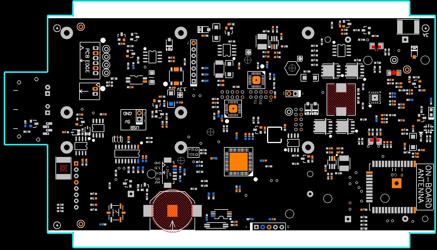
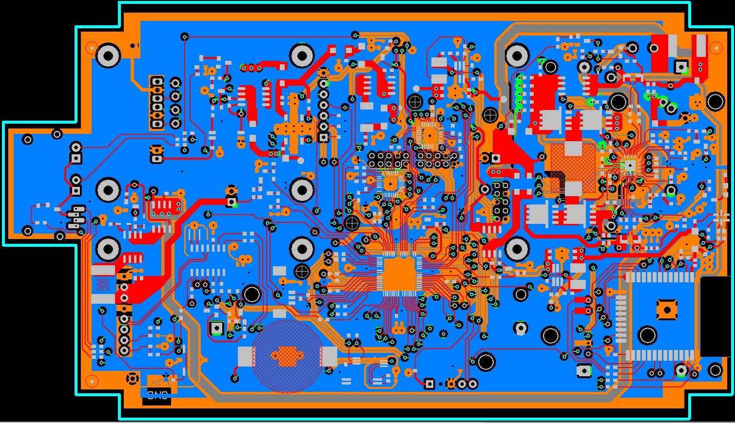
PCB design is the “bread and butter” of our business. We have taken part in thousands of design projects for hundreds of customers, and virtually all of them involved a PCB design phase.

Each design project we work on follows the same overall process.

We start with a review of your project's requirements, which can include:

Review project requirements, which ca n include:

We've started projects based on:

Analysis Phase

Analyze available board area, layer stackup and specialized component / routing needs in order to determine the complexity of the layout Provide you with a reasonable price, either a fixed - bid estimate or a by - the hour estimate

Capture land patterns needed

and arrange them in a rough draft placement within the mechanical outline for the layout

Route critical signals

and signals requiring specialized routing

Adjust the placement of any non-critical components to optimize the route

Conduct a comprehensive review

Run design rule checks, addressing any electrical shorts or borderline-acceptable routes

Generate gerbers, drill files

Submit PCB design file, gerber files, drill files to your engineering staff for a comprehensive review